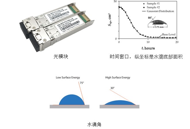
The packaging process of optical modules is similar to that of chip packaging. While reducing the volume, the packaging form will require higher requirements for processes such as solidification and soldering.
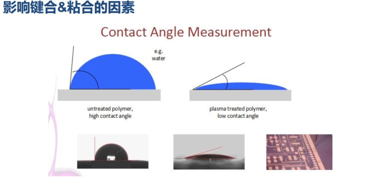
After plasma cleaning activation, the adhesion degree of the chip on the substrate is higher, and the bonding strength between the product pads and gold wires is greater, which improves the sensitivity, emission eye diagram, optical module failure analysis and other performance of the product, greatly improving the production efficiency and yield of the product. Suitable for common packaging products such as QSFP AOC and CPF.