Application of plasma cleaning in Mini&Micro LED packaging:
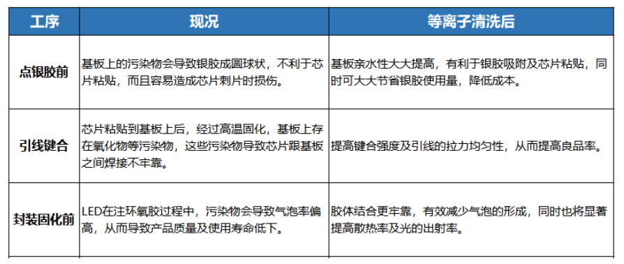
1、 Before packaging with silver adhesive: greatly improve the surface roughness and hydrophilicity of the workpiece, which is conducive to the flat application of silver adhesive on the substrate and chip, and can greatly save the amount of silver adhesive used and reduce costs;
2、 Pre wire cleaning: Clean the solder pads, improve welding conditions, enhance wire reliability and yield;
3、 Plastic sealing: Improve the reliability of non product bonding of plastic sealing materials and reduce the risk of delamination;
4、 BGA substrate cleaning: Performing plasma surface treatment on the pads on the PCB before BGA mounting can achieve the effects of cleaning, roughening, and activating the pad surface, greatly improving the success rate of BGA mounting;
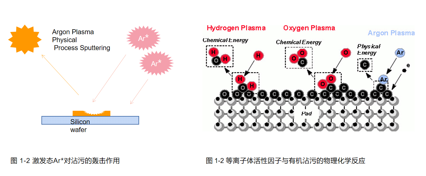
5、 Flip Chip lead frame cleaning: Plasma treatment can achieve ultra purification and activation of the lead frame surface, improving the bonding quality of the chip.
6、 Sealing process: Through plasma surface treatment, especially in the processes of point lens glue, dam filling, and full surface coating, organic dirt on the surface of the product can effectively improve the process pain points such as insufficient fluidity, adhesion, and difficulty in coating between the glue and the substrate or chip.