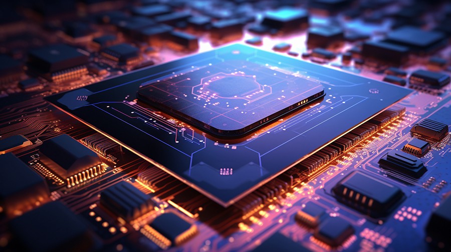
Xinrui Plasma Equipment focuses on advanced semiconductor packaging and assembly (ASPA), wafer level packaging (WLP), and microelectromechanical (MEMS) assembly processes. Plasma applications include cleaning, wire bonding improvement, slag removal, bump adhesion, stripping, and etching.
1. Cleaning and removal of organic pollutants
Plasma equipment can remove oxides, fluorides, etc. Before entering the next process, the Bond Pad needs to remove organic pollutants and other contaminants from the surface. In our equipment chamber, the process gas introduced can be ionized through radio frequency or microwave sources, and many ion free radicals generated can react chemically with pollutants to form new volatile molecules, thus achieving the purpose of cleaning.
2. Surface cleaning (Mold, WireBond, etc.)
During the chip packaging process, plasma cleaning of the Bond Pad before WireBonding is a basic and necessary procedure to improve cleanliness. After cleaning with vacuum plasma equipment, it can be observed that the tension and shear forces of the wire being drawn have been significantly improved.
3. Surface activation (FlipChip Underfill)
Nowadays, whether using general packaging technology or flip chip packaging technology, plasma cleaning of the encapsulated object is required before filling the packaging with compounds. RF or microwave plasma cleaning equipment can perfectly activate and adjust all sizes of surfaces (including gaps) before chip packaging according to production requirements.
4. Wafer surface treatment (cleaning/activation)
Plasma treatment is often used to optimize the interface conditions on the wafer surface, making the interface conductive or insulating. Semiconductors, glass, quartz, and even plastic materials can actively respond to the activation reaction of plasma, thus being better bonded.